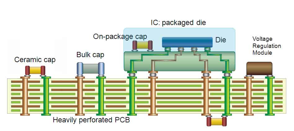
嵌入式和扇出晶圆级封装技术的发展历程 中英文版 高清电子书 Advances in embedded and fan-out wafer level packaging technologies
pcb设计之旁路技术
Introduction
Bypassing and decoupling are subjects that are rarely, if ever, covered in the classroom; but are emphasized in nearly ALL Data Sheets & Application Notes !
The legacy of this is that many new engineers and some technicians ignore it, but they do so at their peril; it is the single greatest reason for prototype hardware debugging problems!
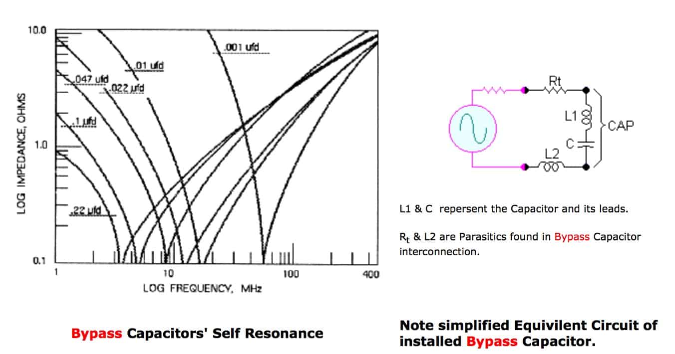
WHAT IS BYPASSING?
When powering any active device, there is one overriding requirement: that the point of entry of the power supply (Power Rail) be as LOW an impedance (relative to ground) as possible, i.e., ideally: zero ohms! This will help to insure the stability of the circuit: Circuit Integrity.
WHY DO WE BYPASS?
The reason for bypassing is to prevent unwanted communications between different devices (or different stages of the same device) that share the same power rail. Also, implicit in this requirement, is the reduction of NOISE present on that power rail–at all frequencies.
HOW DO WE BYPASS?
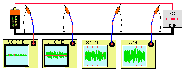
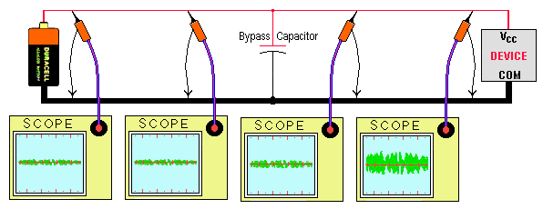
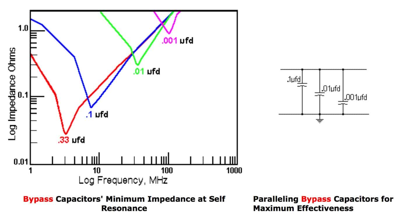
Something as simple as placing a bypass capacitor between power and ground (Vcc and Gnd) of each active device, will effectively restore this nearly ideal power supply–zero ohms output impedance!
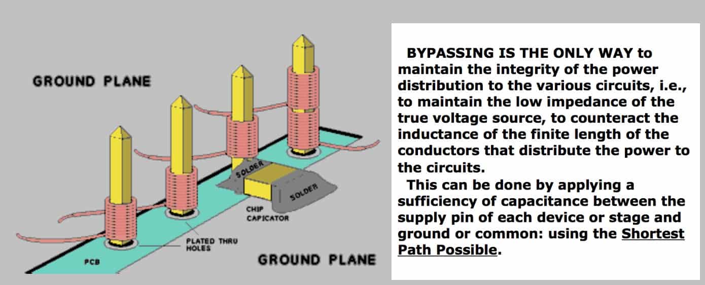
Note how the Bypassing becomes more effective as the ground conductor approaches a continuous plane. Ground planes are often used in high frequency circuit boards for this reason.
Power Rails
Because there is distance between any power source and the active device it powers, a conductor, wire, or trace of finite length is required between that power source and device.
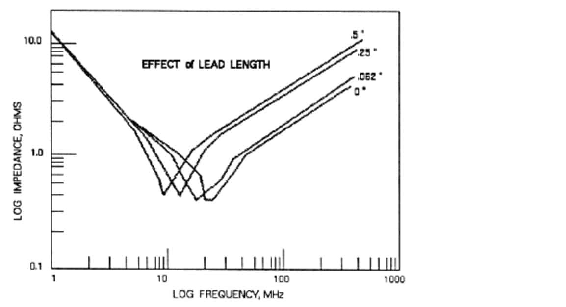
Any conductor, wire, or trace has the properties of resistance and inductance; both can cause problems where power is concerned. The resistance problem can be overcome by increasing the cross-sectional area of the conductor; however, the inductive property is another story.
Even what might appear to be a small inductance, at high frequencies, or very high frequencies, can translate to an unacceptable high impedance. See the figure below:
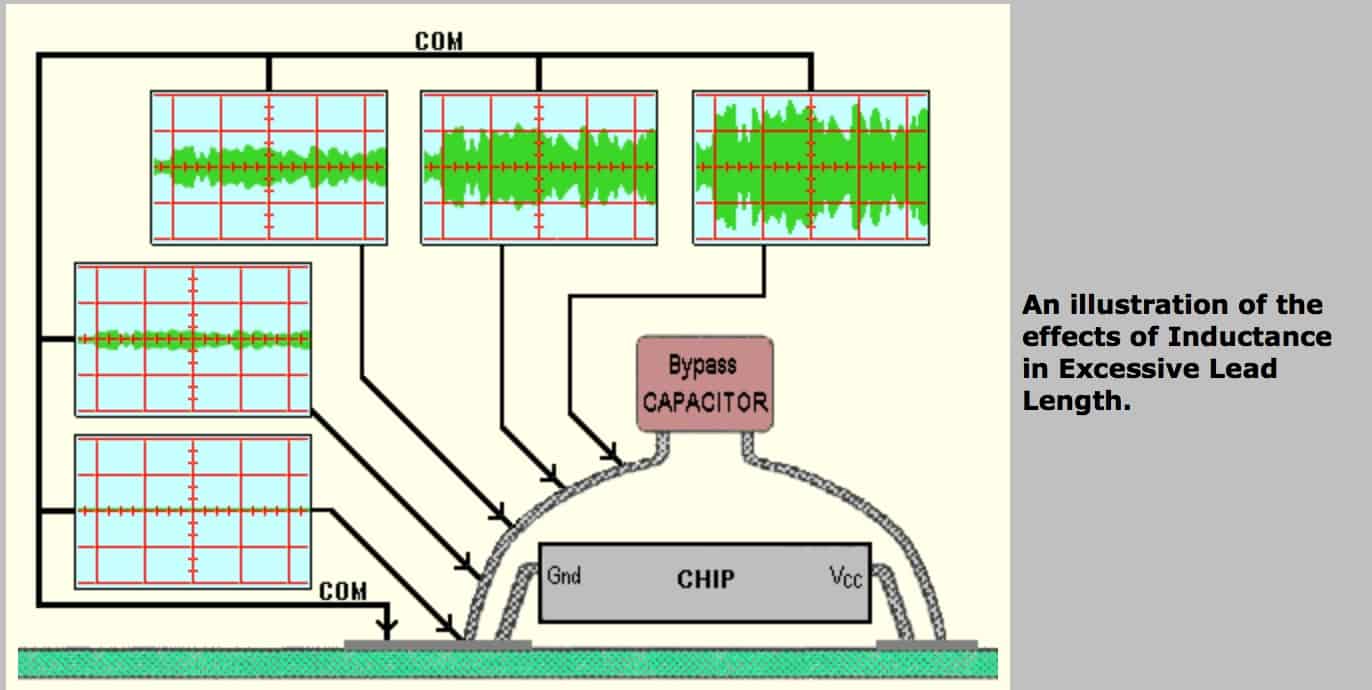
Notice how the Inductive Reactance (XL) of the finite length conductor effects this Zero Ohms Impedance. Hence the active device’s need for varying rates of current creates more NOISE as the conductor length (and the reactance) increases.
Adding a Bypass Capacitor to this Inductive Reactance helps to restore the (virtual) Zero Ohms Impedance.
At this point, it is worth noting that ALL active devices have inputs and outputs–but you already knew that didn’t you! What you may not have considered is that the power rail–the Vcc pin–can be both, an input and output “port.” You only have to examine the schematic of such devices to see that the power rail is common to both input and output stages, i.e., the bias resistors of the input stage are connected to the same “Rail” as the load resistors of the output stages.
This arrangement is not a Bad Thing, because it presupposes that this common power rail will always be held at Zero Ohms! That is, it will be sourced by an Ideal Voltage Source.
Amplifier with various degrees of Power Supply Stabilization in the form of Bypass & Decoupling
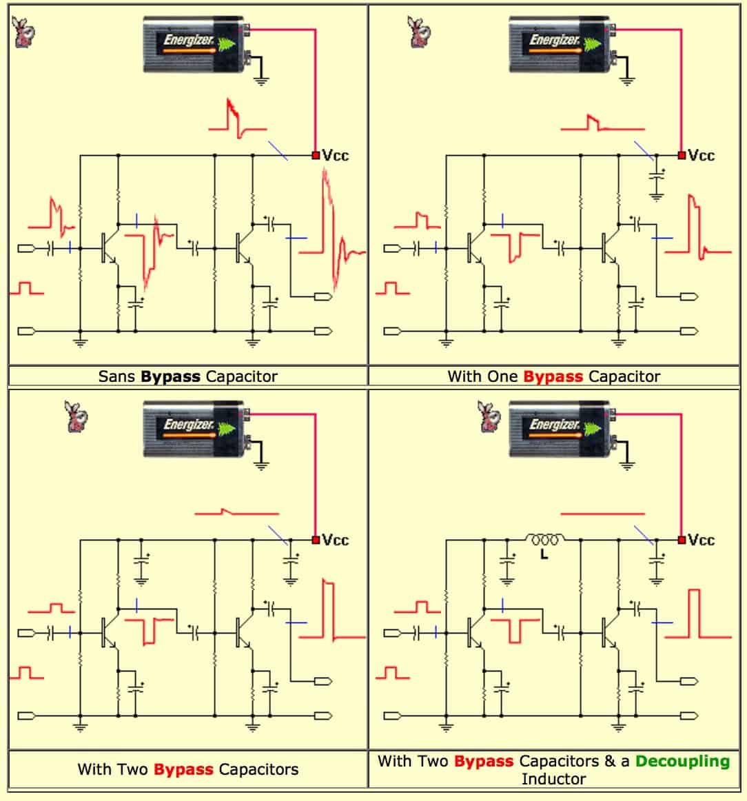
Notice how the power rail–Vcc pin–can be both, an input and output “PORT.”
TTL
TTL (Transistor Transistor Logic) logic is ONE GREAT SOURCE OF NOISE.
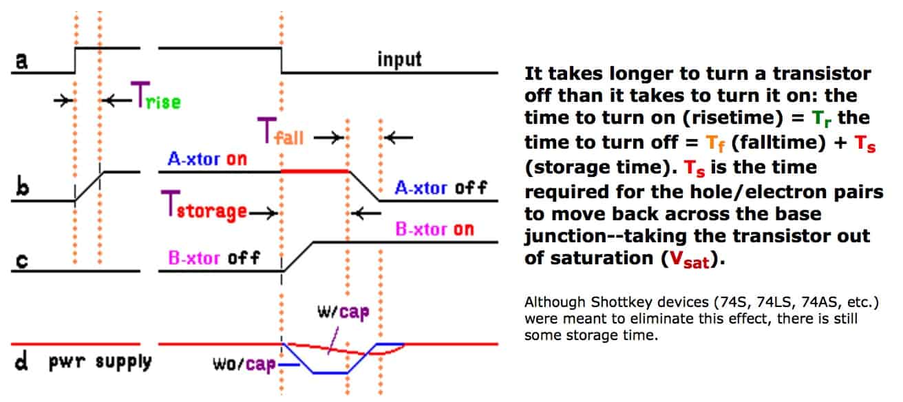
In a typical TTL logic device (gate, flip flop, counter, register, etc.), it is fair to say that at any one time: half of the transistors are ON, and the other half are OFF. However, during logic transitions, for a very short time ALL of the transistors are ON.
TTL is a “Saturating Logic,” i.e., a transistor is either fully off or fully on, and when it is fully on it is said to be, in Vsat.
A saturated transistor requires more time to become unsaturated than it took to become saturated in the first place; this time difference is called storage time (Ts).
Therefore, during any logic transition (one/zero or zero/one) All of the transistors are ON for this short time (Ts)–drawing ~twice its normal current. This latency can last from two or three nanoseconds to as long as fifteen nanoseconds–depending on the logic family.
See the figure below:
In systems using thousands, to hundreds of thousands of gates, there can be a tremendous demand on the power supply, i.e., supplying a constant, non-varying Vcc to a load that is random and very high speed (fast di-dt, i.e., a large current change in a short period of time).
If one could supply power to all of the logic devices at a constant Vcc, everything would be Peachy Keen. However, Life–and Murphy, do not allow anything dealing with engineering design, to be Peachy. –Bummer!
As mentioned previously:
Because there is “Distance” between any power source and the logic it powers, a conductor, wire, or trace of finite length is required between this power source and the logic.
Any conductor, wire, or trace have the properties of resistance and Inductance; both can cause problems where power is concerned. The resistance problem can be overcome by increasing the cross-sectional area, however, the Inductive property is another story.
Even what might appear to be a small inductance, at high frequencies, or very high frequencies, can translate to an unacceptable high impedance.
As in the case of the amplifier, above, TTL logic devices have inputs and outputs; and the power rail–the Vcc pin–can be both, an input and output “port.” Again, an examination of the circuit reveals that the power rail is common to both input and output stages, i.e., the bias resistors of the input stage are connected to the same “Rail” as the load resistors of the output stages.
This arrangement, again, presupposes that this common power rail will always be held at Zero Ohms! That is, it will be sourced by an Ideal Voltage Source.
RECAP
In the world of fast edge sensitive logic, it is a simple matter to conceive of “inappropriate communications” between logic devices (& elements within a device) through the unprotected, high impedance power rail–Vcc.
Because of the speed of this demand on the power supply–Rise and Fall times in the nanoseconds–the frequencies are in the many hundreds of MHz. And, any conductor, be it printed circuit trace, or wire, any conductor, between the device power pin and the power source can look like an unacceptably high resistance–tens of Ohms to hundreds of Ohms.
Something as simple as placing a capacitor between Vcc and ground of each logic device, will effectively create this near Ideal power supply–Zero Ohms output impedance!


4 Comments
头痛
看到一堆英语 头痛
谢谢关注 O(∩_∩)O~
很好的旁路技术总结